Structural Analysis of Lead Sulphide Thin Films Prepared by Pulsed Laser Deposition
Sanjeev Kumar
Sanjeev Kumar*
Department of Physics, Rajiv Gandhi University, Doimukh-791112, Arunachal Pradesh, India
- *Corresponding Author:
- Sanjeev Kumar
Department of Physics, Rajiv Gandhi University, Doimukh-791112, Arunachal Pradesh India
Tel: +91 360 2277569
Fax: +91 360 2277684
E-mail: sanjeev.dr@gmail.com
Received date: Sep 02, 2015, Accepted date: Oct 27, 2015, Published date: Nov 05, 2015
Citation: Kumar S. Structural Analysis of Lead Sulphide Thin Films Prepared by Pulsed Laser Deposition. Nano Res Appl. 2015, 1:1.
Abstract
Effects of the substrate temperature on structural and optical properties of the PbS thin films synthesized using pulsed laser deposition are investigated. The main focus of the present study is to optimize various parameters for good quality films. The study reveals the preferred orientation of (200) reflection plane with compressive stress (-0.31211 GPa) at only 200oC substrate temperature. However, the lowest roughness of the film is also observed at 200oC by using atomic force microscope. Only reflectance spectra are used to determine the band gap of these films in weak absorption region.
Introduction
Thin films are used or applied to an almost limitless range of applications i.e., optical devices, mirrors, semiconductor devices, magnetic media, food wrap, etc. The ability to verify quality is critical to correlating performance of the thin films. Thin films of IV-VI compounds have been considered as the most attractive in semiconductors technology, because of their various applications in the infrared technology. These materials are produced in the crystalline and polycrystalline forms and used as detectors, emitters, as well as solar control coatings [1–5]. Because of the presence of π–π narrow band gap (0.41 eV) in PbS semiconductor [6-9], exhibits its importance in highly efficient photovoltaic conversion devices, optical switching, and related photoelectric devices [10].
The PbS among the lead salt family materials is known as a famous compound and is used as IR detector. This material is fabricated mostly in the form of sensitized polycrystalline film. In the last decade, many research works have been conducted to prepare and increase the photoconductive properties of lead sulfide thin films [11–13]. The development of laser technology has opened up new applications for these compounds. The laser diodes based on lead chalcogenides and their alloys are important sources for the tunable radiations in the mid infrared wavelength region. They are considered to be advantageous for detecting hydrocarbon pollutants in atmosphere, high resolution spectroscopy, trace gas analysis and optical fiber communication system over super long distances [14,15]. The issues for maintaining the stiochiometry can be resolved by using the Pulsed Laser Deposition method to fabricate to make it more effective material [16-18]. However, PbS shows a lower crystalline, therefore films are highly defective and their structural properties are mainly linked to the growth processes used for the layer deposition [19,20]. The target ablated by laser can create a highly energetic growth precursor, leading to non equilibrium growth conditions. Therefore high quality films can be obtained at a fairly low substrate temperature.
In the present study, PbS thin films are deposited using pulsed laser deposition (PLD) technique, in order to maintain the stoichiometry of ablated target into the deposited layer [21-23]. The present study mainly focuses on the investigation of the substrate temperature on the crystalline quality and the surface morphology.
Experimental Details
The UV–PLD is performed with a KrF laser which operates at 248 nm with a repetition rate of 10 Hz and flux density 3.5 J/cm2. PbS films were deposited on corning glass substrates by ablating stoichiometric home-made targets. Pressure was maintained 10-5 torr during the film deposition on different substrate temperature (100, 200,300, 400 and 500°C). In order to investigate the effect of substrate temperature on the surface stress, and structural properties of PbS thin film, a series of samples were deposited at different substrate temperature. X-ray diffraction analysis was performed by using Bruker D8 Advance diffractometer using CuKα (λ=1.54 Å) radiation. Surface morphoclogy and roughness of the deposited films were studied using atomic force microscopy (NT-MDT Ntegra). Room temperature reflectance spectra were measured in the spectral range from 300 to 2500 nm using a UVVis- NIR spectrophotometer (Varian Cary 5000).
Results and Discussion
Figure 1(a) shows the XRD patterns of the PbS films which are deposited at different substrate temperature of 100oC-500oC and compare with PbS powder . All the samples revealed the growth of cubic phase but with different growth directions as the former depicted the growth along (a00) and along (ab0) directions and later (abc) direction (PCD no 5-0692). The effect of the substrate temperature on the lattice constant (a), particle size and stress has been obtained by the XRD shown in Table 1. Lattice parameter for cubic phase structure was calculated using the equation a = d(h2 + k2 + l2)1/ 2, where d is the interplanar distance and a is the lattice parameter. The XRD spectra is used to calculate the size of the particles with increase in temperature by using Sherrer’s formula [24]. We have also incorporated the instrumental broadening (~ 0.1°for microcrystalline Si powder) for the size calculations to estimate maximum particle size 57 nm. The lattice parameter and particle sizes as a function of substrate temperature are shown in Figure 2. The internal stress in the film has been calculated by the relation 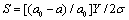 , where a0 and a0 are the lattice parameters of the thin film samples and bulk samples, respectively. We considered the powder sample as the bulk sample. Y and σ are the Young’s modulus and Poisson's ratio of the bulk sample, respectively. For PbS, the value of Y is 70.2 GPa and σ is 0.28 [24].

Figure 1 X-ray diffraction Pattern of PbS powder and thin films at different substrate temperature.

Figure 2 Particle size and lattice constant of PbS powder and thin films at different substrate temperature. 0oC represents the powder sample in this figure.
| Sample | Particle Size | lattice Constant | Stress |
|---|---|---|---|
| Powder | 23 | 5.9444 | - |
| 100°C | 40 | 5.9084 | 1.51836 |
| 200°C | 16 | 5.9518 | -0.31211 |
| 300°C | 36 | 5.9156 | 1.21468 |
| 400°C | 45 | 5.9048 | 1.67019 |
| 500°C | 57 | 5.912 | 1.36652 |
Table 1: The effect of the substrate temperature on the lattice constant (A), particle size and stress has been obtained by the XRD.
The XRD peak intensity is observed to increase with increase in substrate temperature as expected. However at temperature 200°C preferred (200) orientation peak with maximum intensity has been observed at the cost of disappearance of (111) reflection plane with the fact that PbS grew along (200) plane that possess lowest surface energy for cubic structure. Therefore, the growing film develops a crystallographic structure with minimum total energy of the system and expect to have fast grain growth of stable nuclei along (200) and it attributes to the fact that 10-50% of the atoms are surface atoms. Due to large fraction of these surface atoms, the contribution of surface energy dominates the overall energy of the system that favors the high energy configuration. It also may be the compressive stress at this particular temperature due to the differences in mechanical and thermal properties that exist between the film and substrate. This compressive stress may be the reason for small grain size because if compressive stress applied the lattice spacing it used to decrease lattice space for the plane perpendicular to the stress direction and increase for plane parallel to the stress direction. The (111) plane has been reappeared at 300°C substrate temperature and reaches maximum intensity at 500°C with decreasing the (200) reflection peak intensity, which may be due to lattice spacing increase for perpendicular in the stress direction as seen in the Table 1.
Grains have been counted at the surface of the film by the NOVA software after analysis of the AFM images, taken by the NTGARA MDT Scanning probe microscope and depicted in Figure 3. These results show the morphology of the film surface at different substrate temperatures. We count the less number of the grains on the surface of the film fabricated at 200°C, which indicates the high surface density of fine particle because of negative thermal stress. That could be the reason of low surface roughness on the surface. Fig 3F shows the roughness increasing after 200°C substrate temperature.

Figure 3 (A,B,C,D and E): Mapping of AFM Images to count the grains at different Substrate Temperature (A) 100 (B) 200 (C) 300 (D) 400 (E) 500 and (F): Roughness of film Vs Substrate Temperature.
Figure 4 shows the optical reflection spectra of PbS films deposited by PLD at different substrate temperatures. The reflection spectra have been taken between a wide range of the spectrum and divided into three regions (i.e., Strong absorption, Absorption and Weak absorption) to understand the behavior of films in each region. While during the increase in temperature the grain boundary are formed by clusters and droplets in the processes of film deposition. These grain boundaries give rise to the internal scattering of light on the surface. As shown in the Figure 4 increasing in the temperature the reflectance intensity in all regions decreases that can be attributed to the increased surface roughness with increase in substrate temperature. Figure 5 show the band gap has been calculated by using reflection spectra of weak absorption region using Tauc Relation. A graph between  has been plotted, where α is proportional to
 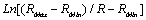 , where the reflectance falls from Rmax to Rmin due to the absorption by the thin film material and R is the reflectance for any intermediate energy photons. So, we have used α in the terms of reflectance as
  [25]. A very small change has been found in the energy band gap (Eg), which shows that the substrate temperature has no much effect on the thickness and other electronic parameters of the film but it has considerable influences on structural parameters (like surface roughness and morphology) . It has been observed that the band gap (Eg ~0.5 eV ) for all films is close to the value of bulk lead sulphide (0.44eV) [23], which might be due to quantum confinement.

Figure 4 Reflectance spectra of lead sulphide at different substrate temperature in different regions.

Figure 5 Band gap calculation of lead sulphide film by only reflectance in weak absorption region.
Conclusion
The influence of the substrate temperature on Pulse laser deposited Lead Sulphide polycrystalline film has been observed in this work. 200°C temperature has been found as the optimized temperature for a good quality film of lead sulphide fims. Effect of substrate temperature on band gap of these films has been found negligible after determined by only reflection spectra with high reflectivity of the optimized film.
Acknowledgement
Author would like to acknowledge to Dr Ramesh Chandra, IIC IIT Roorkee for his support and cooperation.
References
- Slonopas A,Alijabban N, Saltonstall C, Globus T, Norris P (2015) Electrochimica Acta 151:140.
- Agne M, Lambrecht A, Schiessi U, Tacke M (1994) Infrared SciTechnol 35-47.
- Snaith HJ, Stavrinadis A, Docampo P, Watt AAR(2014) Solar Energy 85: 1283.
- Rogalski A (2012) Opto-Electronics Review. 20: 279
- Thargaraju B, Kaliannan P (2000) SemicondSci Technol 15: 849.
- Brown PR, et al. (2014) ACS Nano 8: 5863.
- Malyarevich AM, et al.(2001) Phys Status Solidi b 224:253
- Ellingson RJ, et al. (2005) Nano Lett 5:865.
- Krauss TD, Wise FW (1997) Phys Rev B 55:9860.
- Slonopas A,Alijabban N, Saltonstall C, Globus T, Norris P (2014) Electrochimica Acta 151:140
- Kotadiya NB, Kothari AJ, Tiwari D, Choudhuri TK (2012) Applied Phys A 108: 819.
- Safrani T, et al. (2014)J Mater Chem C 2: 9132
- Pusio J, Tamulevicius S, Lindroosh S, Lakela M (2003) Thin Solid Films 426: 223.
- Abbe S, Furukawa Y, Mochizuki K, MasumatoK (1994) J Jpn Inst Metals 58: 346.
- Lambrecht A, Kurbel R, Agne M (1993) Mater Sci Eng 21: 217.
- Ullrich B, Sakai H, Segawa Y (2001) Thin Solid Films 385: 220.
- Liu GZ, Lei QY (2012) Appl Phys Lett100: 202902
- Hillie KT, Curren C, Swart HC (2001) Appl Surf Sci 177: 73.
- Gunasekaran M, Ichimura M (2005) Jap J Appl Phys 44: 7345.
- Schenck PK, Vaudin MD, Bonnell DW, Hasti JW, Paul AJ (1998) Appl Surf Sci 655: 127.
- Weber MJ (2003) Hand Book Optical Materials. CRC Press 117.
- Kumar S, et al. (2014) J Apl Phys116: 073504
- Kumar S, Khan ZH, Majeed Khan MA, Husain M (2005) Current Applied Physics 5: 561
- Elements of X-ray diffraction by Cullity 1956 (academic press)

Open Access Journals
- Aquaculture & Veterinary Science
- Chemistry & Chemical Sciences
- Clinical Sciences
- Engineering
- General Science
- Genetics & Molecular Biology
- Health Care & Nursing
- Immunology & Microbiology
- Materials Science
- Mathematics & Physics
- Medical Sciences
- Neurology & Psychiatry
- Oncology & Cancer Science
- Pharmaceutical Sciences