The Modified Electrode Position of Uniform and Defect-free TiO2 Nanolayer onto Stainless Steel Substrate with Enhanced Photocatalytic Performance
Masood Hamadanian, Hani Sayahi, Alireza Zolfaghari and Vahid Jabbari
Masood Hamadanian1,2, Hani Sayahi2, Alireza Zolfaghari3 and Vahid Jabbari4*
1Institute of Nano Science and Nano Technology, University of Kashan, Kashan, Iran
2Department of Physical Chemistry, Faculty of Chemistry, University of Kashan, Iran
3Department of Physical Chemistry, Chemistry and Chemical Engineering Research Center of Iran, Tehran, Iran
4Department of Chemistry, The University of Texas at El Paso, El Paso, Texas 79968, USA
- *Corresponding Author:
- Vahid Jabbari
Department of Chemistry, The University of Texas at El Paso, El Paso, Texas 79968, USA
Tel: +98 31 55912382
Fax: +98 31 55912397
E-mail: vjabbari86@gmail.com
Received date: Aug 02, 2015, Accepted date: Oct 15, 2015, Published date: Oct 20, 2015
Citation: Hamadanian M, Sayahi H, Zolfaghari A, et al. The Modified Electrode Position of Uniform and Defect-free TiO2 Nanolayer onto Stainless Steel Substrate with Enhanced Photocatalytic Performance. Nano Res Appl. 2015, 1:1.
Abstract
The photocatalytic behavior of photocatalyst TiO2 nanolayers which were fabricated via a modified electrodeposition method in a nonaqueous media, have characterized in comparison to microlayers. The electrodeposition applied voltage and the electrodes distance were taken as control parameters to obtain the layers in the nanoscale thicknesses. The existence of TiO2 in the deposited sample was confirmed by energy dispersive X-ray analysis (EDAX) technique. The surface uniformity of the fabricated layers was studied by scanning electron microscopy (SEM). Both atomic force microscopy (AFM) images and ellipsometric analysis of the deposited films confirmed the nanometric thicknesses of the prepared oxide layers. The fabricated samples demonstrated high photocatalytic activity under UV irradiations. This functionality along with physical and chemical stability of the fabricated layers makes it possible to consider as a powerful photocatalyst in degradation of pollutants.
Keywords
TiO2; Electrodeposition; Thickness control; Nanolayer; Photocatalysis
Introduction
Heterogeneous photocatalysis has attracted attentions as an alternative or complementary technology for degradation of dissolved pollution in aqueous environments [1-3]. During photocatalysis process, usually a source of UV radiation is used to stimulate the photocatalyst material and caused the oxidation of pollutant on the surface of oxidant layers [4]. Among the most commonly used photocatalysts, titanium oxide (TiO2) has been widely investigated in wastewater treatments [5-7], due to the high oxidation ability, biocompatibility for living organisms, and low price. It is usually preferred to use as particulate TiO2 thin film photoelectrodes because it provides suitable specific surface area that is necessary for acceptable photocatalytisis activity [8- 11]. Furthermore, the troublous separation processes that are required when using suspensions of nanoparticles are avoided [12]. Synthetic control of the formation of TiO2 films has been proved to be important in improving the functional properties [11,12].
In order to improve photocatalytic activity of TiO2 films for technical applications, two principle strategies should be considered during fabrication process. First, the synthetic films should have reasonable physical and chemical stability in water treatment plants. Second, the cost of procedure should be low along suitable photocatalysis property. The photoactivity of oxide layer is expressed by quantum efficiency, which is related to the width of depletion layer and the film thickness [13]. Theoretical studies and our reported paper have shown that decreasing the film thickness gives the photogenerated electron-hole pairs more chance to avoid recombination processes and this means an increase in quantum efficiency [12,13].
Many methods have been used to deposit the TiO2 thin film onto a substrate, such as dry methods, i.e., chemical vapor deposition (CVD) [14,15], sputtering [16], and wet methods i.e., sol–gel [17], self-assembled monolayers (SAMs) [18-20], liquid phase deposition (LPD) [21-24] and electrochemical methods [25-28]. Recently, the electrochemical fabrication of TiO2 layer onto foreign substrates has attracted more attention, due to its highly controllable and low cost process [29-31]. It means that the characteristic states of the films can be easily controlled by varying the preparation conditions, such as potential, distance between electrodes and current density during electrochemical deposition [25]. These general advantages of electrochemical methods along with some special characteristics of the proposed procedure (thickness control and stability of the layers) make it attractive to develop for industrial purposes.
In the present work, which to best of our knowledge was done for first time in such a comprehensive exploration, a modified electrodeposition method was used to prepare nanolayers of TiO2 onto stainless steel electrodes as foreign substrate. In order to compare our results with a reference study, the layers also were prepared by Kamada method [25]. The widely usage, low cost and high chemical and mechanical stability of stainless steel in industries were the motivation to choose it as the main substrate. The thickness of TiO2 was controlled by electrodeposition potential, electrodes distance and the concentration of water in non-aqueous electrolyte. Also, photocatalytic efficiency of the fabricated films was examined using photo-degradation of aqueous solution of methylene blue (MB) as probe pollution.
Experimental
Electrodeposition of TiO2 nanolayers onto the steel substrate
All chemicals were purchased from Merck Co and used without further purification. The stainless steel with an area of 78 cm2 and thickness of 0.5 mm, cut from a standard sheet of stainless steel 304, were used as substrate. Before the electrodeposition of the oxide layers, standard procedures of degreasing and pickling were performed [25].
All electrodeposition experiments were carried out in a two electrode cell. Titanium foil (Alfa Aesar 4 × 2 cm2, thickness 0.15 mm) and prepared stainless steel sheet were used as a sacrificial anode and prepared cathode electrodes, respectively. Generally, the distance between these electrodes was restricted to 0.5 cm, but the effect of distance was also studied on the quality of the deposited layers. The nonaqueous electrolyte was consisted of I2 (1 g/l) as a supporting electrolyte in acetone solvent and a small amount of water (<1%). The electrodeposition was carried out under a constant potential ranging from 5 V to 15 V, with 5 V intervals, at room temperature. The usage of water up to 1% results in a layers within micrometer ranges. Finally, the fabricated layers were annealed at 600ºC for 30 min in Ar ambience.
Characteristic
The uniformity and the morphology of the deposited films were observed by scanning electron microscopy, SEM, (PHILIPS, XL30) and atomic force microscopy, AFM, (DME, DSM45). The compositions of the deposited films were analyzed by elemental analysis, utilizing EDAX (PHILIPS, XL30). Thickness analysis of the layers which were prepared by electrodepositon and Kamada methods were examined by spectroscopic ellipsometer (SENTECH, SE 800) and surface profilometer (DECTAK 3) respectively. The photocatalytic activity of the deposited films was evaluated for the decomposition of MB analyzed by a spectrophotometer (Agilent-8453E). Due to avoid errors in our results, the synthesis and characterization processes of the prepared layers were repeated for several times.
Results and Discussion
Fabrication
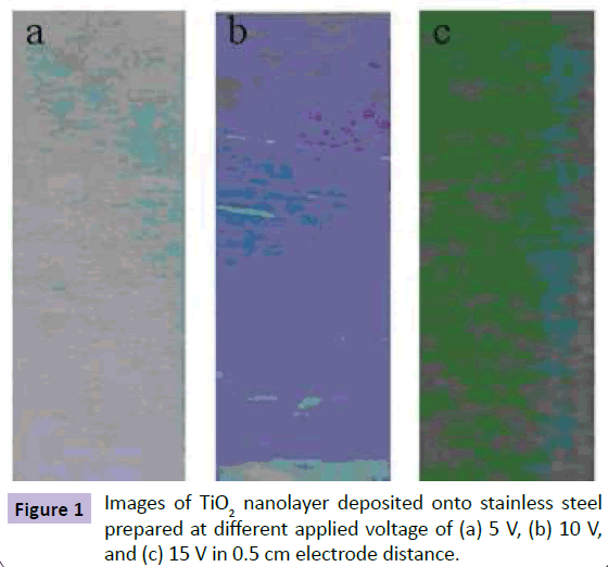
After electrodeposition at 5, 10 and 15 V for 30 min, various colors of the oxide layers were appeared onto the cathodes electrode (steel), and the anode electrode (titanium) changed from colorless to tinge of brown (Figure 1). As the employed potential increased up to 15 V, the hydrogen gas which rising from the cathode prevents the electrodeposition of TiO2 layer uniformly. Figure 1 shows the various colors of the fabricated oxide layers at different voltages. The colors were originated from the diffraction of the incident light on the surface of the oxide layers. The fact that the thicker layers diffract the incident light more [32,33], results in a wide range of spectra for different thicknesses. It should be mentioned that these iridescent spectras are specific characteristics of nanometric TiO2 layers [32,33]. The results of ellipsometery measurement have shown that thicknesses of prepared nanolayer at 5, 10, 15 V applied voltage were 291, 231 and 196 nm, respectively [34,35]. The layers which are prepared by Kamada methods were semitransparent which is characteristic of layers with thicknesses of micrometer (~1 μm) [25].
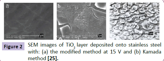
SEM was used to study the uniformity of the samples. As it is shown in Figure 2, some cracks were appeared on the surface of the TiO2 layers. In fact, evaporation of residual solvents can lead to cracks due to contraction of the thin films [36]. In Figure 2(b), the cracks in the TiO2 layer prepared using Kamada method are deeper and clearer than electrodeposited TiO2 nanolayers. The significant crack formation in Kamada method is in result of higher amount of the water in electrolyte (1% <) compared to our electrolyte. The excess water causes increasing in Ti foil corrosion and as a result, thick layer even in low potential and electrodeposition time are resulted. On the other hand, the hydrogen evolution on the cathode, due to the presence of excess water, prevented the layer to be deposit uniformly.
Physical and chemical stability of the fabricated TiO2 nanolayers were contrasted with the TiO2 layers prepared by Kamada method [25]. Indeed, the brittle semitransparent white films prepared by the Kamada method completely delaminated by the first touching, but the nanolayers fabricated by our procedure have been stable in aqueous phases even under vigorous shaking. On the other hand, the samples which prepared with Kamada method aren't suitable for liquid phases and will be overwhelm with a little movement. Chemical resistance of the TiO2 nanolayers was tested by using various concentrations of HCl solutions. The chemical stability of prepared layer was investigated by corrosion test and the obtained results exhibited a high chemical stability of the prepared nanolayers.
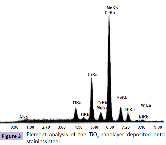
Figure 3 shows the element analysis results of the TiO2 nanolayer onto stainless steel substrate by electrodeposition method (<1% water).Element analysis with EDAX confirms the existence of TiO2 in the deposited sample. In fact, due to low thicknesses of electrodeposited nanolayers in comparison with Kamada method, XRD pattern couldn't prove the TiO2 structures even after annealing the electrodeposited layers. Due to, the low thicknesses of electrodeposited nanolayers, the TiO2 peaks were not obvious because of overlapping by peaks of stainless steel elements. Therefore, the EDAX pattern was more suitable analysis method to indicate existence of TiO2 onto the stainless steel substrate.
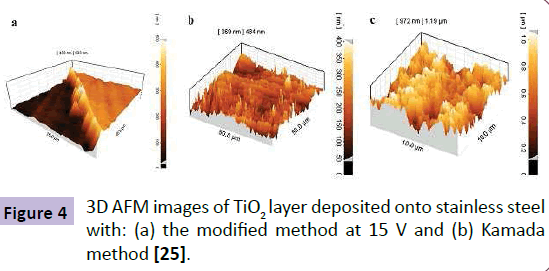
Figure 4 shows the 3D AFM images of TiO2 nanolayers deposited onto the stainless steel electrode. Figure 4(a) is related to the electrodeposited TiO2 nanolayer with modified electrodepostion method. The area with deposited oxide layer is brighter than the bare stainless steel surface. The results show that the formed layer has around 300 nm thicknesses. Figures 4(b) show the AFM image of TiO2 microlayers which were prepared by Kamada method [25]. As shown in Figure 4, TiO2 layer prepared with our proposed method results in more uniform and defect free films comparing to the Kamada layer.
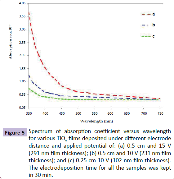
To consider the effect of different factors, namely the applied voltage and electrode distance, during the electrodeposition process of TiO2 nanolayers, ellipsometric analysis of deposited films were carried out. The results exhibited that more voltage applied leads to thicker films and samples prepared, for example, under 15 v applied voltage were obviously thicker than those prepared under 10 v applied voltage. The distances between the cathode and anode electrodes in electrodeposition process is a highlighted point to be considered. Fitting the electrodes in 0.5 cm distance yielded the thickest and the most uniform films. Both decreasing and increasing of this space was resulted in some nonuniformities and thinner films which is due to higher solution resistance in higher distances between electrodes. Figure 5 shows the absorption coefficient dependency of the prepared samples to the wavelength of the incident light which was measured by ellipsometry spectroscopy [34,35]. As mentioned before, clearer and thicker films show higher absorption coefficients.
Figure 5 Spectrum of absorption coefficient versus wavelength for various TiO2 films deposited under different electrode distance and applied potential of: (a) 0.5 cm and 15 V (291 nm film thickness); (b) 0.5 cm and 10 V (231 nm film thickness); and (c) 0.25 cm 10 V (102 nm film thickness). The electrodeposition time for all the samples was kept in 30 min.
Photocatalytic Activity
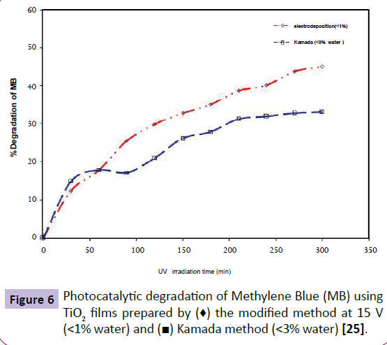
Photocatalytic activity of TiO2 layer deposited by our proposed method (15 V, 30 min) and Kamada methods onto stainless steel were analyzed by degradation of 30 ml of MB (2 ppm) aqueous solution (Figure 6). As shown in Figure 6, the sample that was prepared by our modified process has shown superior photocataytic activity than Kamada sample, in spite of its lower thickness. The removal efficiency of TiO2 nanolayer prepared under 15 v applied voltage was around 45% in 300 min irradiation time. Further, it should be considered that the stability of the Kamada method-based prepared sample is less than those of nanolayers. In addition, although the Kamada method-based prepared film was immersed with utmost care in the solution, TiO2 layer was delaminated gradually. Therefore, it has made many problems in dissociation of TiO2 particles from the operation environment.
Conclusion
In the current study, a simple electrodeposition method was proposed and used to fabricate uniform TiO2 nanolayers with high chemical resistance and excellent photocatalytic activity. The thicknesses of TiO2 film prepared by electrodeposition which are reported by previous studies were mainly in the range of a few micrometers. Here, we have shown that decreasing the water extent in the electrolyte along with applying lower range of potentials, about 15 v, can result in thinner nanometric films. Due to, the fabricated films were physically stable in aqueous environment, they could be used as photocatalytic electrodes in aqueous mediums including dissolved pollutant. This might be thought as powerful aspect of this modified method to be developed and expended into the industrial applications.
Acknowledgement
This work was supported by the Iran government grant and also, Authors gratefully acknowledges the financial support from Iran Initiative Council of Nanoscience and Nanotechnology.
References
- Song L, Zeng X, Zhang X (2011) Photocatalytic Activities of TiO2 Modified by Poly (fluorene-co-bithiophene) under Visible Light. Energy Procedia 11: 2162-2168.
- Didier R, Sixto M (2002) Solar photocatalysis: a clean process for water detoxification. Science of The Total Environment 291: 85-97.
- Bougheloum C, Messalhi A (2009) Photocatalytic Degradation of Benzene Derivatives on TiO2 Catalyst. Physics Procedia 2: 1055-1058.
- Aguado J, van Grieken R, Lopez-Munoz MJ, Marugan J (2002) Removal of cyanides in wastewater by supported TiO2-based photocatalysts. Catalysis Today 75: 1-4.
- Hoffmann MR, Martin ST, Choi W, Bahnemann DW (1995) Environmental Applications of Semiconductor Photocatalysis.Chem Rev 95: 69-96.
- Stafford U, Gray KA, Kamat PV (1994) Radiolytic and TiO2-Assisted Photocatalytic Degradation of 4-Chlorophenol. A Comparative Study J Phys. Chem 98: 6343-6351.
- Linsebigler AL, Lu G, Yates JT (1995) Photocatalysis on TiO2 Surfaces: Principles, Mechanisms, and Selected Results Chem Rev 95: 735-758.
- Kim SK, Chang H, Cho K, Kil DS, Cho SW, et al.(2011) Enhanced photocatalytic property of nanoporous TiO2/SiO2 micro-particles prepared by aerosol assisted co-assembly of nanoparticles. Materials Letters 65: 3330-3332.
- Zaben A, Aruna ST, Tirosh S, Gregg BA, Mastai Y (2000) The Effect of the Preparation Condition of TiO2 Colloids on Their Surface Structures. J PhysChem B 104: 4130-4133.
- Ma Y, binQiu J, Cao Y, Guan ZS, Yao JN (2001) Photocatalytic activity of TiO2 films grown on different substrates. Chemosphere 44: 1087-1092.
- Hamadanian M, Behpour M, Razavian AS, Jabbari V (2011) Structural, Morphological and Photocatalytic Characterizations of Ag-Coated Anatase TiO2 Fabricated by Sol–Gel Dip-Coating Method. Journal of Experimental Nanoscience.
- Zolfaghari A, NasiriAvanaki K, Jooya HZ, Sayahi H (2007) Optimization of the operational controlling parameters in indirect photocatalytic oxidation of water dissolved pollutants on nanostructured TiO2 thin film electrodes. Semicond Sci Technol 22: 653-657.
- Soedergren S, Hagfeldt A, Olsson J, Lindquist SE (1994) Theoretical Models for the Action Spectrum and the Current-Voltage Characteristics of Microporous Semiconductor Films in Photoelectrochemical Cells. J PhysChem 98: 5552-5556.
- lee WG, Woo SI, Kim JC, Choi SH, Oh KH (1994) Preparation and properties of amorphous TiO2 thin films by plasma enhanced chemical vapor deposition. Thin Solid Films 237: 105-111.
- Schuisky M, Harsta A, Aidla A, Kukli K, Kiisler AA, et al.(2000) Atomic Layer Chemical Vapor Deposition of TiO2 Low Temperature Epitaxy of Rutile and Anatase. J Electrochem Soc 147: 3319-3326.
- Mardare D, Tasca M, Delibas M, Rusu GI (2000)On the structural properties and optical transmittance of TiO2 r.f. sputtered thin films. Applied Surface Science 156: 200-206.
- Yu J, Zhao X, Zhao Q (2000) Effect of surface structure on photocatalytic activity of TiO2 thin films prepared by sol-gel method. Thin Solid Films 379: 7-14.
- Shin H, Collins RJ, De Guire MR, Heuer AH, Sukenik CN (1995) Synthesis and characterization of TiO2 thin films on organic self-assembled monolayers: Part I. Film formation from aqueous solutions. Journal of Materials Research 10: 692-698.
- Lin H, Kozuka H, Yoko T (1998) Preparation of TiO2 films on self-assembled monolayers by sol–gel method. Thin Solid Films 315: 111-117.
- Xiao Z, GuJ, Huang D, Lu Z, Wei Y (1998) The deposition of TiO2 thin films on self-assembly monolayers studied by X-ray photoelectron spectroscopy. Applied Surface Science 125: 85-92.
- Shimizu K, Imai H, Hirashima H, Tsukuma K(1999) Low-temperature synthesis of anatase thin films on glass and organic substrates by direct deposition from aqueous solutions. Thin Solid Films 351: 220-224.
- Kishimoto H, Takahama K, Hashimoto N, Aoi Y, Deki S (1998)Photocatalytic activity of titanium oxide prepared by liquid phase deposition (LPD). J Mater Chem 8: 2019-2024.
- Deki S, Aoi Y, Hiroi O, Kajinami A (1996) Titanium (IV) Oxide Thin Films Prepared from Aqueous Solution.Chem Let 25: 433-437.
- Lee MK, Lei BH (2000) Characterization of Titanium Oxide Films Prepared By Liquid Phase Deposition Using Hexafluorotitanic Acid. Japanese Journal of Applied Physics 39: 101-106.
- Kamada K, Mukai M, Matsumoto Y (2002) Electrodeposition of titanium (IV) oxide film from sacrificial titanium anode in I2-added acetone bath.ElectrochimicaActa 47: 3309-3313.
- Kavan L, O’Regan B, Andreas K, Gratzel M (1993) Preparation of TiO2 (anatase) films on electrodes by anodic oxidative hydrolysis of TiCl3. Journal of Electroanalytical Chemistry 346: 291-307.
- Matsumoto Y, Adachi H, Hombo J (1993) New Preparation Method for PZT Films Using Electrochemical Reduction. J Am Ceram Soc 76: 769-772.
- Zhang X, Yao B, Zhao L, Liang C, Zhang L, et al.(2001) Electrochemical Fabrication of Single-Crystalline Anatase TiO2 Nanowire Arrays. J ElectrochemSoc 148: G398-G403.
- Natarajan C, Nogami J (1996)CathodicElectrodeposition of Nanocrystalline Titanium Dioxide Thin Films. J Electrochem Soc 143: 1547-1552.
- Karuppuchamy S, Amalnerkar DP, Yamaguchi K, Yamaguchi T, Sugiura T, et al. (2001) Cathodic Electrodeposition of TiO2 Thin Films for Dye-Sensitized Photoelectrochemical Applications. Chemistry Letters 30: 78-79.
- Ishikawa Y, Matsumoto Y (2001)Electrodeposition of TiO2 photocatalystinto nano-pores of hard alumite.Electrochim Acta 46: 2819-2824.
- Li Y, Ishigaki T (2002) Thermodynamic analysis of nucleation of anatase and rutile from TiO2 melt. J Crystal Growth 242: 511-516.
- Hrapovic S, Luan BL, D’Amours M, Vatankhah G, Jerkiewicz G (2001) Morphology, Chemical Composition, and Electrochemical Characteristics of Colored Titanium Passive Layers. Langmuir 17: 3051-3060.
- Debora G, Eugene I (2002) Fundamentals and applications of spectroscopic ellipsometry. Quim Nova 25: 794-800.
- Fujiwara H (2007) spectroscopic ellipsometery: principles and applications.firstEdn, John Wiley and Son.
- Yamazaki H, Tsuyama T, Kobayashi I, Sugimori Y (1992) Preparation of Pb (Zr, Ti)O3 Thin Films Using All Dipivaloylmethane Source Materials by Metalorganic Chemical Vapor Deposition.Jpn J Appl Phys 31: 2995-2997.
Open Access Journals
- Aquaculture & Veterinary Science
- Chemistry & Chemical Sciences
- Clinical Sciences
- Engineering
- General Science
- Genetics & Molecular Biology
- Health Care & Nursing
- Immunology & Microbiology
- Materials Science
- Mathematics & Physics
- Medical Sciences
- Neurology & Psychiatry
- Oncology & Cancer Science
- Pharmaceutical Sciences
